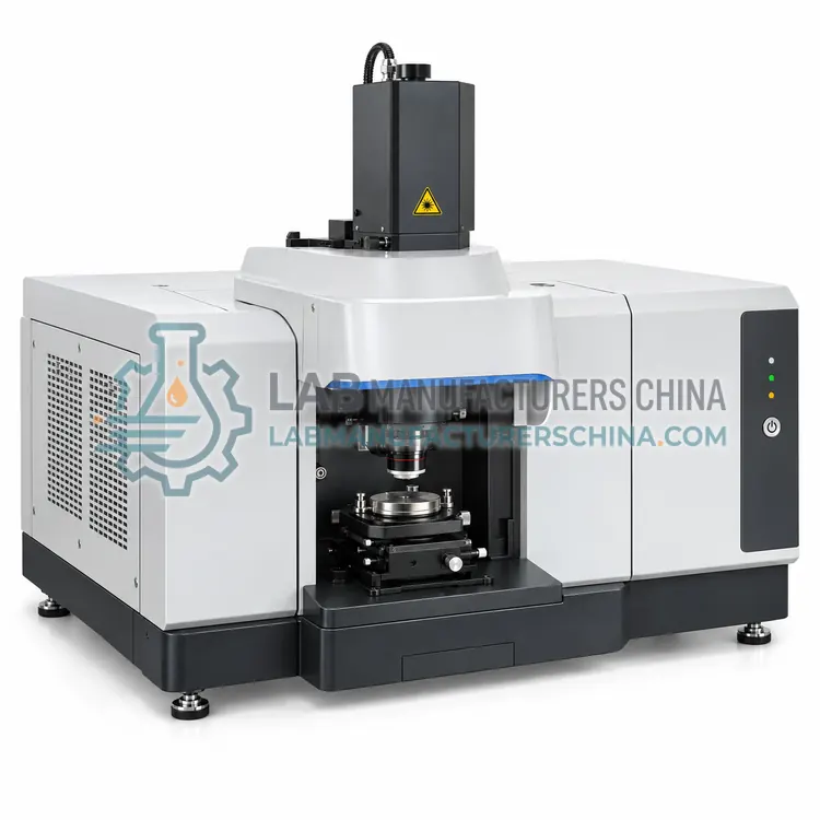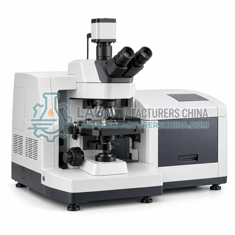
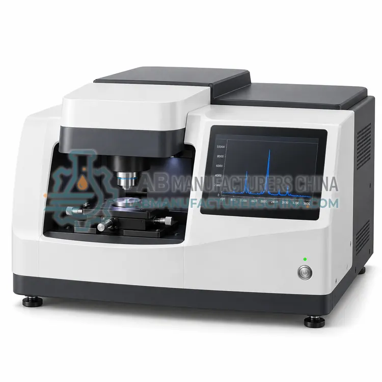
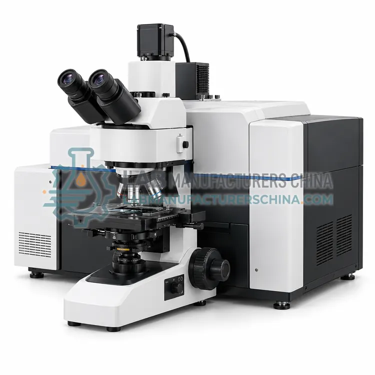
Confocal Raman Microscope
共聚焦拉曼显微镜
- SKU RAM-0002
- Raman
- CE (to be confirmed)
- IEC 60825-1 (to be confirmed)
- ISO 9001 manufacturing (to be confirmed)
Price on request — FOB / CIF quoted per order
Prices depend on configuration, quantity and destination port.
Key specifications
| Laser wavelengths | 532, 633, 785 nm (selectable) |
|---|---|
| Spatial resolution (lateral) | ≤0.5 µm (532 nm, 100× objective) |
| Axial resolution | ≤2 µm (confocal) |
| Spectral resolution | 0.3–4 cm-1 (grating dependent) |
| Spectral range | 50–4000 cm-1 |
| Lowest wavenumber | ≤10 cm-1 (with filters) |
Request a quote Download brochure · to be provided
By Lab Manufacturers China Technical TeamLast reviewed Standards: ASTM E1840, ASTM E2529, ASTM E2911
What is the Confocal Raman Microscope?
A confocal Raman microscope couples a Raman spectrometer with a research microscope to obtain spectra and chemical maps at micrometer spatial resolution. It is the suitable choice for particles, inclusions, thin films and layered materials, with depth resolution of about 1–2 µm.
What is the Confocal Raman Microscope?
A confocal Raman microscope couples a Raman spectrometer with a research microscope to obtain spectra and chemical maps at micrometer spatial resolution. It is the suitable choice for particles, inclusions, thin films and layered materials, with depth resolution of about 1–2 µm.
Overview
The confocal Raman microscope focuses the laser through a 100× objective to a spot of about 0.5–1 µm and collects the scattered light through a confocal pinhole, which rejects out-of-focus signal and gives axial resolution of 1–2 µm. Motorized XYZ stages allow point analysis, line scans, area mapping and depth profiling. Multiple lasers, often 532, 633 and 785 nm, are selected by software, and the spectrograph typically has 300–2400 gr/mm gratings with focal lengths of 250–800 mm for resolution of 0.3–4 cm-1. Mapping of a 100 × 100 µm area at 1 µm steps is possible in minutes with fast electron-multiplying CCD detection. Applications include polymorph mapping in tablets, graphene layer counting, semiconductor stress, geological inclusions and microplastics. Sample damage and heating at high laser density require power control.
How does it work?
When monochromatic laser light hits a sample, most photons scatter elastically, but about one in 10 million scatters inelastically with an energy shift equal to a vibrational energy of the molecule. This Raman shift, reported in cm-1, produces a spectrum of peaks characteristic of chemical bonds and crystal structure. A Raman spectrometer consists of a laser such as 532, 633, 785 or 1064 nm, focusing and collection optics, a notch or edge filter that rejects Rayleigh scattering, a dispersive spectrograph with CCD detector or an FT interferometer, and software. Shorter laser wavelengths give stronger signals but can excite fluorescence, while 785 and 1064 nm reduce fluorescence at lower signal. Polarization, confocal pinholes and surface enhancement increase selectivity and sensitivity, and calibration with standards such as silicon at 520.7 cm-1 and acetaminophen ensures accurate shifts.
What are the key features?
- Confocal pinhole provides 1–2 µm depth resolution and rejects out-of-focus signal.
- Automated switching among 532, 633 and 785 nm lasers.
- Motorized XYZ stage supports point, line, area and depth mapping.
- Multiple gratings from 300 to 2400 gr/mm balance coverage and resolution.
- EMCCD or cooled CCD detection enables fast mapping at low laser power.
- Polarization optics and low-wavenumber filters reach below 10 cm-1.
What are the technical specifications?
A typical confocal raman microscope configuration offers laser wavelengths of 532, 633, 785 nm (selectable), spatial resolution (lateral) of ≤0.5 µm (532 nm, 100× objective), axial resolution of ≤2 µm (confocal), spectral resolution of 0.3–4 cm-1 (grating dependent), spectral range of 50–4000 cm-1 and lowest wavenumber of ≤10 cm-1 (with filters). Values are indicative of the product class; the exact figures for each configuration are confirmed on the quotation and the calibration documents supplied with the instrument.
Which applications is it used for?
The Confocal Raman Microscope is used in polymorph and excipient mapping in tablets, graphene and 2D material characterization, semiconductor stress and composition, geological inclusion analysis and microplastic particle identification. Across the wider Raman class, laboratories also deploy it for pharmaceutical raw material identification, polymorph and API form analysis and carbon nanomaterials and graphene characterization.
Which standards and certifications apply?
Relevant standards and methods include ASTM E1840, ASTM E2529, ASTM E2911, USP <1120>, Ph. Eur. 2.2.48, IEC 60825-1 and ISO 17025. Certification candidates for this model are CE, IEC 60825-1 and ISO 9001 manufacturing; each is to be confirmed for the specific configuration before shipment, and certificates are supplied only where they have been issued.
Operate Raman systems in rooms with controlled ambient light or use an enclosed sample compartment, since stray light raises the baseline. Treat lasers according to IEC 60825-1 classifications and use interlocks and protective eyewear where open beams are possible. Check wavenumber calibration daily with silicon and intensity response with a standard material, and track laser power drift. Avoid burning dark or absorbing samples by reducing power and using rastering or defocusing. Cooled CCD detectors need stable temperature, and dust should be kept off optics. Maintain spectral libraries and validate identification methods against known references, especially for regulated raw material identification.
How do I select the right Confocal Raman Microscope?
Select the confocal Raman microscope when spatial resolution, depth profiling or mapping is needed. For bulk identification of homogeneous samples, a benchtop or handheld unit is more economical. In an RFQ, specify lasers, gratings, spatial and depth resolution, stage travel, detector type and mapping software.
How does it compare with other Raman variants?
Choose a Raman spectrometer based on the sample's fluorescence behavior, spatial scale and operating environment. Laser wavelength is the first decision: 532 nm for strong signal from inorganics and carbon, 785 nm for general organics and pharmaceuticals, and 1064 nm for highly fluorescent or colored samples. Bulk identification can use a benchtop or handheld instrument, while samples smaller than 100 µm or requiring depth profiling and mapping need a confocal Raman microscope. Process monitoring requires a fiber-optic probe and a robust enclosure. Compare spectral resolution of 2–6 cm-1, spectral range, laser power, detector cooling and library options. Consider laser safety class, sample heating risk and compliance with 21 CFR Part 11 in regulated laboratories.
Full specifications
| Laser wavelengths | 532, 633, 785 nm (selectable) |
|---|---|
| Spatial resolution (lateral) | ≤0.5 µm (532 nm, 100× objective) |
| Axial resolution | ≤2 µm (confocal) |
| Spectral resolution | 0.3–4 cm-1 (grating dependent) |
| Spectral range | 50–4000 cm-1 |
| Lowest wavenumber | ≤10 cm-1 (with filters) |
| Objectives | 5×, 20×, 50×, 100× |
| Stage travel | ≥75 × 50 mm, 0.1 µm step |
| Detector | Cooled CCD or EMCCD |
| Mapping speed | ≥100 spectra/s (fast mode) |
Indicative values for this product class. Final specifications are confirmed on the quotation and in the calibration documents supplied with the instrument.
Applications
- Polymorph and excipient mapping in tablets
- Graphene and 2D material characterization
- Semiconductor stress and composition
- Geological inclusion analysis
- Microplastic particle identification
Key features
- Confocal pinhole provides 1–2 µm depth resolution and rejects out-of-focus signal.
- Automated switching among 532, 633 and 785 nm lasers.
- Motorized XYZ stage supports point, line, area and depth mapping.
- Multiple gratings from 300 to 2400 gr/mm balance coverage and resolution.
- EMCCD or cooled CCD detection enables fast mapping at low laser power.
- Polarization optics and low-wavenumber filters reach below 10 cm-1.
Frequently asked questions about Confocal Raman Microscope
A confocal pinhole in the collection path blocks light from outside the focal plane, so signal comes mainly from a small volume of roughly 1 µm laterally and 2 µm axially. This allows depth profiling and improves spectra from layered or fluorescent samples.
Yes. The positions and intensity ratio of the G and 2D peaks near 1580 and 2700 cm-1, together with the D peak, allow layer number and defect density estimation for graphene. Excitation wavelength and power must be controlled to avoid heating.
Mapping speed depends on signal strength. Fast modes with EMCCD or line-focus illumination acquire around 100 spectra per second, so a 100 × 100 pixel map takes a few minutes, while weak scatterers can require seconds per point.
Raman spectroscopy identifies materials from their vibrational fingerprint. It is used for raw material identification, polymorph screening, carbon nanomaterial characterization, mineral and gemstone ID, forensic analysis and process monitoring, and it often works through glass or plastic containers.
Use 532 nm for strong signals from inorganics and carbon, 785 nm as a good balance for organics and pharmaceuticals, and 1064 nm to avoid fluorescence in colored or biological samples. Shorter wavelengths give stronger scattering, since intensity scales with 1/λ4.
Fluorescence is usually much stronger than Raman scattering and produces a broad background that can swamp Raman peaks. Switching to a longer excitation wavelength, using photobleaching, time gating or baseline correction reduces this interference.
Related models