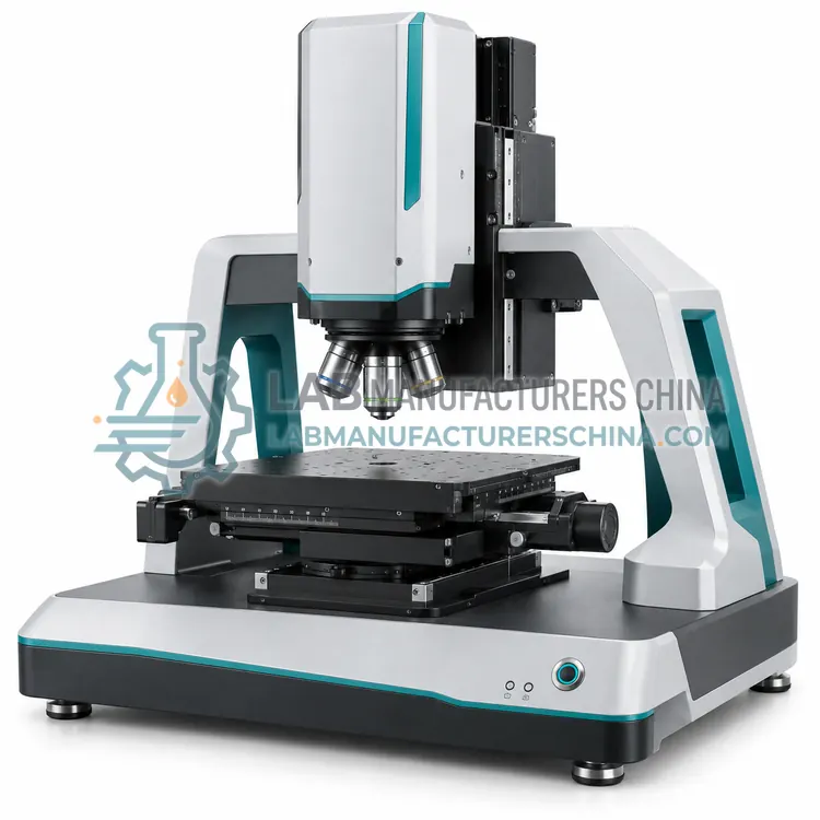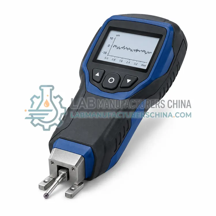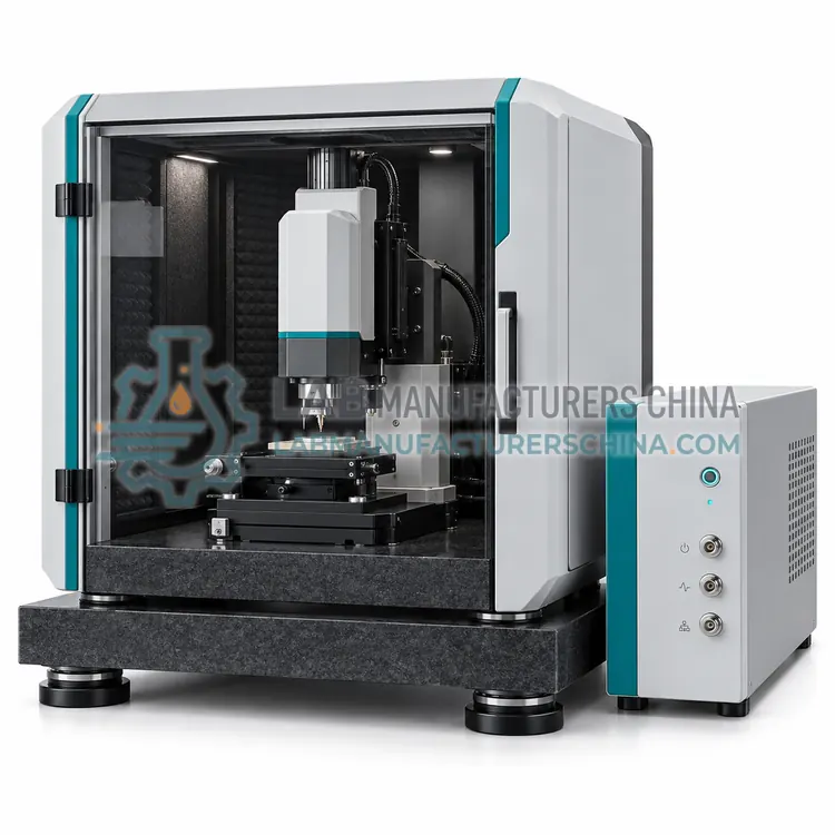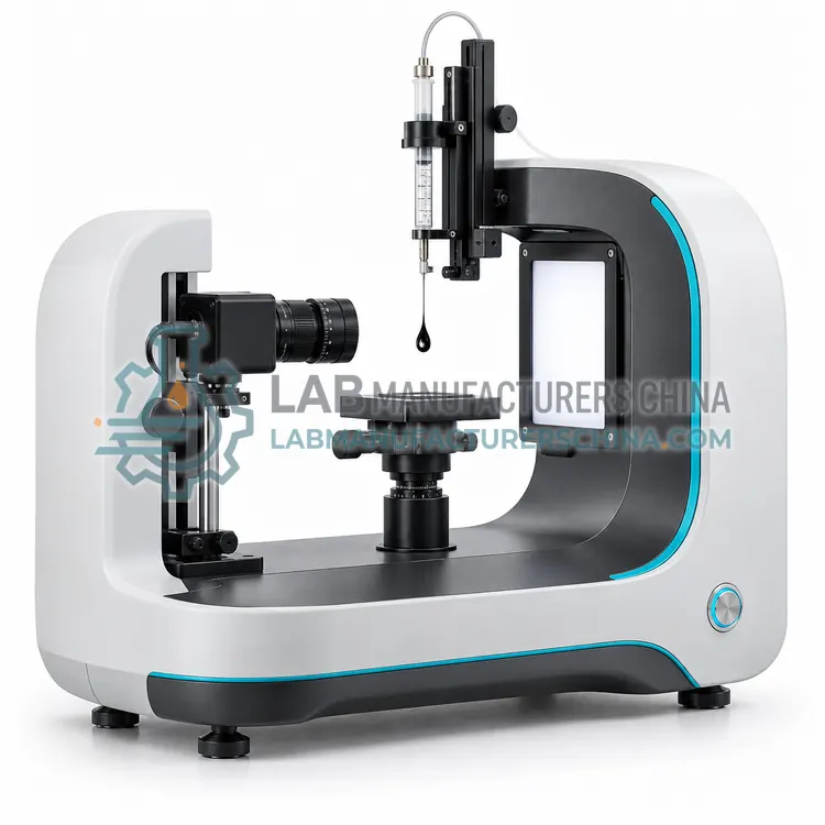
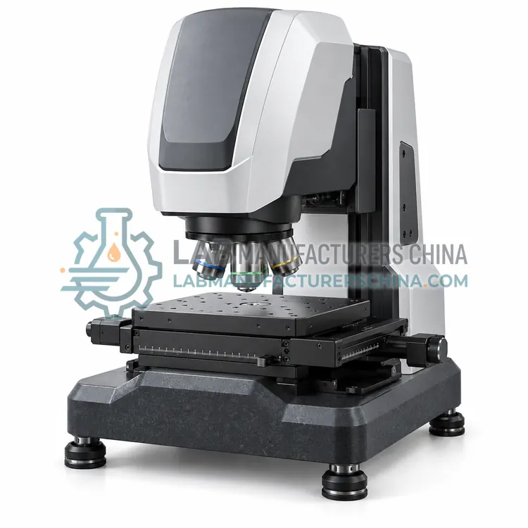
White-Light Interferometric 3D Optical Profilometer
白光干涉三维光学轮廓仪
- SKU SUP-0002
- Surface Profilometers
- CE (to be confirmed)
- ISO 9001 manufacturing (to be confirmed)
- Laser/LED safety classification (to be confirmed)
Price on request — FOB / CIF quoted per order
Prices depend on configuration, quantity and destination port.
Key specifications
| Vertical resolution | < 0.1 nm (PSI); ~1 nm (CSI) |
|---|---|
| Vertical scan range | Up to 10 mm |
| Objectives | 2.5×–100× |
| Field of view | 0.05–5 mm |
| Lateral resolution | 0.35–4 µm (objective-dependent) |
| Camera | 1–5 MP |
Request a quote Download brochure · to be provided
By Lab Manufacturers China Technical TeamLast reviewed Standards: ISO 4287, ISO 21920-2, ISO 25178-2
What is the White-Light Interferometric 3D Optical Profilometer?
A non-contact profiler using vertical scanning white-light interferometry to map areas with sub-nanometer vertical resolution and Sa, Sq and step height outputs. It is the right choice for smooth surfaces, MEMS, films and optics where contact could damage the sample.
What is the White-Light Interferometric 3D Optical Profilometer?
A non-contact profiler using vertical scanning white-light interferometry to map areas with sub-nanometer vertical resolution and Sa, Sq and step height outputs. It is the right choice for smooth surfaces, MEMS, films and optics where contact could damage the sample.
Overview
A white-light interferometer splits broadband illumination into a reference and a sample beam inside an interferometric objective, such as a Michelson, Mirau or Linnik type. A piezo stage scans the objective vertically while a camera records the fringe intensity at each pixel. The position of maximum fringe contrast gives the height at that pixel. Vertical resolution is below 0.1 nm for phase-shifting mode and about 1 nm in coherence-scanning mode, with scan ranges from a few micrometers to 10 mm. Objectives from 2.5× to 100× provide fields of view from 0.05 mm to 5 mm. Stitching extends areas. Areal parameters from ISO 25178, such as Sa, Sz and Sdr, and step heights are calculated. Steep slopes above about 30° and transparent films need care.
How does it work?
A stylus profilometer drags a diamond tip, usually with a 2 µm or 5 µm radius, across the surface at a constant speed under a small force, and a transducer converts its vertical displacement to an electrical signal. The raw profile is filtered with a Gaussian filter into roughness and waviness using a cut-off wavelength such as 0.8 mm, and parameters such as Ra, Rz and Rq are calculated according to ISO 4287. Optical profilers use white-light interferometry, confocal microscopy or focus variation to determine height at each pixel by analyzing fringe contrast or sharpness while scanning vertically. They produce areal maps with parameters defined in ISO 25178, such as Sa and Sq, without touching the sample.
What are the key features?
- Vertical scanning interferometry with piezo or linear stage
- Turret with 2.5× to 100× interferometric objectives
- Vertical resolution below 0.1 nm in phase-shifting mode
- Automatic stitching for large area and form measurement
- ISO 25178 areal parameter and step height software
- Active vibration isolation table option for stable scans
What are the technical specifications?
A typical white-light interferometric 3d optical profilometer configuration offers vertical resolution of < 0.1 nm (PSI); ~1 nm (CSI), vertical scan range of Up to 10 mm, objectives of 2.5×–100×, field of view of 0.05–5 mm, lateral resolution of 0.35–4 µm (objective-dependent) and camera of 1–5 MP. Values are indicative of the product class; the exact figures for each configuration are confirmed on the quotation and the calibration documents supplied with the instrument.
Which applications is it used for?
The White-Light Interferometric 3D Optical Profilometer is used in MEMS and semiconductor topography, optical surface roughness, polished metal and ceramic analysis and thin film step height. Across the wider Surface Profilometers class, laboratories also deploy it for machined part surface finish, semiconductor film step height and optical component roughness.
Which standards and certifications apply?
Relevant standards and methods include ISO 4287, ISO 21920-2, ISO 25178-2, ISO 4288 and ASTM D7127. Certification candidates for this model are CE, ISO 9001 manufacturing and Laser/LED safety classification; each is to be confirmed for the specific configuration before shipment, and certificates are supplied only where they have been issued.
Place the instrument on a vibration isolation table or heavy bench and away from drafts, since nanometer-level signals are easily disturbed. Calibrate vertical and horizontal scales with certified step-height or roughness standards at defined intervals, and check stylus wear or tip radius regularly. Clean samples before measurement and mount them level. Specify cut-off length, evaluation length and filter type in the method, because Ra depends on them. Keep stylus force low for soft materials and inspect for scratches. Optical systems need objective cleaning and periodic lateral calibration with grid standards.
How do I select the right White-Light Interferometric 3D Optical Profilometer?
Select this variant for smooth or delicate surfaces that need areal 3D data, nanometer resolution and no contact. It is less suited to very rough, steep or opaque-sparkling surfaces where a confocal or stylus system is better. In an RFQ, specify objectives, scan range, stitching, sample size and vibration isolation.
How does it compare with other Surface Profilometers variants?
The main choice is between contact and non-contact. Stylus instruments are traceable, tolerant of steep flanks and dirt, and are the reference for ISO 4287 roughness on machined parts, but they can scratch soft surfaces and cannot reach features smaller than the tip radius. Optical profilers map areas quickly, suit delicate coatings, MEMS and films, and give 3D parameters, but struggle with transparent, very steep or highly reflective or absorbing surfaces. Consider vertical range and resolution, lateral resolution, scan length, sample size and weight, vibration isolation, software filters, and whether the work follows ISO 21920, ISO 25178 or ASTM D7127. Portable roughness testers suit shop-floor checks.
Full specifications
| Vertical resolution | < 0.1 nm (PSI); ~1 nm (CSI) |
|---|---|
| Vertical scan range | Up to 10 mm |
| Objectives | 2.5×–100× |
| Field of view | 0.05–5 mm |
| Lateral resolution | 0.35–4 µm (objective-dependent) |
| Camera | 1–5 MP |
| Step height repeatability | ≤ 0.1% (1σ) |
| Maximum slope | ≈ 30° (smooth), up to 70° with high NA |
| Sample size | Up to 200 × 200 mm, 100 mm height |
| Measurement time | 5–60 s per field |
Indicative values for this product class. Final specifications are confirmed on the quotation and in the calibration documents supplied with the instrument.
Applications
- MEMS and semiconductor topography
- Optical surface roughness
- Polished metal and ceramic analysis
- Thin film step height
Key features
- Vertical scanning interferometry with piezo or linear stage
- Turret with 2.5× to 100× interferometric objectives
- Vertical resolution below 0.1 nm in phase-shifting mode
- Automatic stitching for large area and form measurement
- ISO 25178 areal parameter and step height software
- Active vibration isolation table option for stable scans
Frequently asked questions about White-Light Interferometric 3D Optical Profilometer
Very steep slopes above about 30° to 70°, strongly absorbing or transparent layers, and very rough surfaces may give missing data or artifacts. Transparent films need modeling or special modes to separate layers.
Phase-shifting interferometry gives sub-angstrom resolution on very smooth surfaces but only over small height ranges. Coherence scanning interferometry uses white-light fringes to measure rough surfaces and large steps with about 1 nm resolution.
Yes, when verified with certified step height and lateral grid standards. Vertical calibration is typically checked annually, and a daily check on a reference step is good practice for critical measurements.
A stylus profilometer physically traces a line with a diamond tip and gives traceable 2D profiles, while an optical profilometer maps an area without contact using interferometry or confocal techniques. Stylus suits machined parts, optical suits delicate or areal analyses.
Ra is the arithmetic mean of absolute profile height deviations from the mean line within the evaluation length, given in micrometers. It is the most common roughness parameter but does not distinguish peaks from valleys, so Rz or Rq may also be reported.
A stylus or optical profiler scans across the edge of a film or etched feature, and the height difference between two levelled reference regions gives the step height. Calibration uses certified step standards, typically from 10 nm to several micrometers.
Related models